Combinational Logic
- Logic without memory
- Out = f(inputs)
- is solely defined by the inputs
Delays
- Gates and signals have propagation delays
- In timing diagrams we use the ideal gate (no delays)
- In reality there is a a delay
- That means in implementation, true combinational circuits do not exist because their value still depends on time
Synthesis
- Given: Specification, Library (and, nor, not, etc)
- Result: A circuit that implements the specification with the library elements
- Steps
- Define the inputs and outputs
- Draw a truth table for every output as a function of all inputs
- Compute the logic expression for every output
- Minimize the expression if needed
- Use available library elements to assemble your circuit (ex: using only NAND)
- Possible transformation needed
- Optimization
- The cost function depends on the design goals and the underlying technology
- Goals
- Monetary cost
- low amount of gates and connections
- low number of inputs per gate
- High speed
- parallel processing
- low number of stages
- Low power
- Monetary cost
Implementation
Structures that can be used to implement logic functions
Custom
Certain logical functions can be custom or semi-custom generated by design software
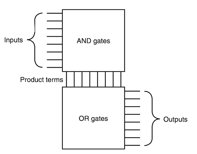
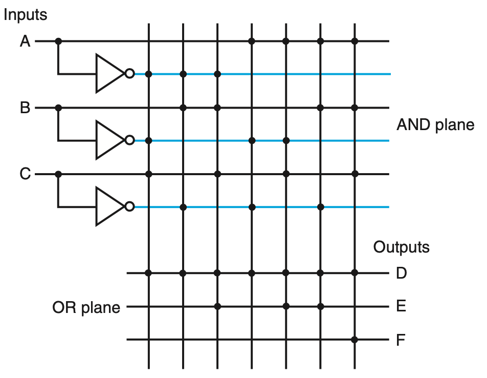
Programmable Logic Array (PLA)
- Implementation of two-level logic
- Advantages
- Only the truth table entries that product a true value for at least one output have any logic gates associated with them
- Each different product term will have only one entry in the PLA
- Structure:
- Often drawn as a grid:
Read-Only Memory
- Has a set of locations that can be read, but are fixed
- Read Only Memory
- Can encode a collection of logic functions directly from the truth table
- Similar to a PLA but fully decoded so it will always contain more entries
- As the inputs grows, the numbers of entries grows exponentially